I. Vacuum application for chip manufacturing
Semiconductors are shaping our world, contributing to every aspect of human welfare. Evolutions like Cell phones, computers, the internet, and social media owe their existence to the advancements in semiconductor technology. The latest trends in Big data and Artificial Intelligence have paved the way for new growth and innovation in the semiconductor market.
Vacuum plays a vital role in realizing the semiconductor chip. From the processing of the initial raw product to the realization of the final chip, various processes involve different levels of vacuum. The various processes involved in the semiconductor industry are
- Deposition
- Etching & Cleaning
- Implantation of lon
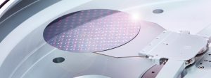
- Handling of Wafers
- Lithography
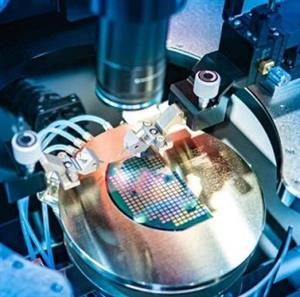
- Wafer Inspection & Metrology

Deposition
Deposition processes create layers of dielectric (insulating) and metal (conducting) materials used to build a semiconductor device. Depending on the type of material and structure being made, different techniques are employed. The various technologies include Physical Vapor Deposition (PVD), Plasma Enhanced Chemical Vapor Deposition (PECVD), Sub-Atmospheric Chemical Vapor Deposition (SACVD), Low-Pressure Chemical Vapor Deposition (LPCVD), and Atomic Layer Deposition (ALD). Each technology requires different levels of vacuum.
The most common PVD method is sputtering technology where the inert gas ions generated by plasma are bombarded on the target material. The combination of dry roughing pumps along with turbo/cryo pumps is best suited for the PVD method.
Plasma-enhanced CVD (PECVD) and ALD are used to form the critical insulating layers that isolate and protect all of these electrical structures. Except for High-Density Plasma deposition (HDPCVD), most of the processes operate under a primary vacuum, in the mbar pressure range
LPCVD applications are typically used in semiconductor manufacturing to create Polysilicon thin films, insulating oxides, or passivation layers. Diffusion is a thermal process used for oxidation and nitration of the wafer surface, or to change the electrical properties of the doped layers.
ALD processes operate under a primary vacuum in the range of 0.1 to 5 mbar. Based on the volume of manufacturing equipment, the capacities of dry pumps can be determined so that faster evacuation with high throughput is ensured.
Etching and cleaning
The etching process results in the creation of chips after selectively removing films and materials that are deposited on the wafer. Strip and clean techniques are used between manufacturing steps to eliminate unwanted material that could later lead to defects and to prepare the wafer surface for subsequent processing. The vacuum requirement for the stripping and cleaning process is in the range of 1 mbar and high-capacity dry pumps are most suited. Due to the absence of load lock chambers in some equipment used in this process, faster pump down times are expected for high throughput
Processes like Dry dielectric etching, Conductor, and Polysilicon etching operate in the range of 0.01 to 0.001 mbar and combinations of turbopumps backed by dry vacuum pumps are mostly suited for this process. Turbopumps are connected to the chamber while dry backing pumps are placed in the basement.
Advanced etch techniques, such as atomic layer etching (ALE) are capable of removing a few atomic layers of material at a time. While conductor etches processes precisely shape electrically active components like transistors, dielectric etch forms the insulating structures that protect conducting parts.
Implantation of lon
A major consideration in chip manufacturing is changing the electrical characteristics of the material and improving the conductivity of the device. As a result, doping the silicon wafer surface with ions is vital. The main areas where the significant contribution of vacuum pumps is observed are Beamline, an End station, and the source.
Ion source operation combines a turbo pump with a dry vacuum pump. For the dry vacuum pump, a leak check is mandatory as this will impact the process’s lifetime. Further process grade N2 purge is mandatory for the operation.
For the beamline area and end station area, turbopumps can be used to provide an absolutely clean environment at a vacuum range of 10-8 mbar.
Handling of Wafers

Process chambers must be under vacuum conditions during the handling of wafers in order to prevent particle contamination. The vacuum level required in the load lock and transfer chambers is in the range of 0.1 to 0.01 mbar. As the requirement is a fast pump down for high throughput, a combination of turbopump with backing dry vacuum pump is recommended for the operation of wafer handling.
Implantation of lon
Lithography is the process of transferring patterns to each layer of the wafer. With the new developments, the chip size is shrinking and new methods of lithography are being introduced. Some of the technologies are Deep Ultra Violet (DUV) technology and Extreme Ultra Violet (EUV) technology. The EUV technology provides better critical dimensions compared to DUV technology. In the EUV light source chamber, the collector mirrors are protected with a very high flow of hydrogen in order to prevent tin deposition. Primary dry vacuum pumps with high hydrogen handling capacities are used for this purpose.
Wafer inspection and metrology
Constant monitoring and metrology are critical as the manufacturing process becomes more and more complex. Dimensional measurements and material analysis are done under vacuum environments where low vacuum is required. For this purpose, turbopumps with backing dry vacuum pumps are recommended.
In addition to the above process, some major points should be taken care of while preparing a semiconductor chip.
- A single leak present on the semiconductor tool or associated process will have a huge impact on the yield.
- At the basement level, dry vacuum pumps and the associated pipings should be cleaned and checked regularly.
II. Hyesungtech J.SC provide vacuum solution
Industrial applications requiring a clean working environment or sub-atmospheric pressure require a steady vacuum supply . Hyesungtech Vietnam J.S.C is a leading enterprise specializing in the vacuum field in Vietnam. With a diverse product portfolio and high expertise, we provide our customers with the most optimal vacuum solutions, ensuring production efficiency, energy saving and environmental protection.
Hyesungtech Vietnam J.S.C are currently the representative distributor of vacuum pump products of European brands: Leybold and Atlas Copco. In addition, we also provide repair services for the world’s leading pump brands such as: Bush; Edward; Ebara; Varian; Ulvac….
In the field of manufacturing electronic components, Hyesungtech Vietnam J.S.C are currently a reliable partner providing vacuum products and services for major corporations in the world: Intel, Seoul Semiconductor, LG, Samsung,….
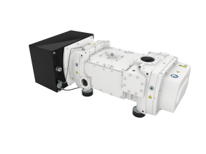
Dry vacuum pump common application in chip production of Leybold that Hyesungtech Vietnam J.S.C is distributing.
 DRYVAC DV 650 S
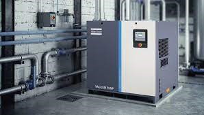
In addition to manufacturing electronic components, GHS VSD+ series of oil-lubricated screw vacuum pumps of Atlas Copco are also always the optimal choice for pick-and-place applications.

CÔNG TY CP HYESUNGTECH VIET NAM
VPGD: Số 3 Ngõ Viện Máy, tổ 21 Phường Mai Dịch, Quận Cầu Giấy, TP. Hà Nội
Miền Nam: 265 Tỉnh lộ 15, Ấp 1, xã Tân Thạnh Tây, Huyện Củ Chi, TP. HCM
Điện thoại: 0972.294.380 (Mr. Thiện) (Zalo; viber; mobi)
Email: thiennguyen@hyesungtech.com.vn
Website: https://vacuumservices.com.vn/
Keywords: Atlat copco, bơm chân không, Chân không.Linh kiện điện tử, Leybold, sản xuất linh kiện điện tử
