Bơm hút chân không cho sản xuất chíp và linh kiện điện tử đóng vai trò then chốt trong hầu hết các công đoạn quan trọng như deposition, etching, quang khắc và vận chuyển wafer... Một hệ thống chân không ổn định, sạch và được thiết kế đúng sẽ đảm bảo chất lượng sản phẩm và năng suất của toàn bộ dây chuyền.
Chân không trong sản xuất chip, linh kiện điện tử gồm những công đoạn nào?
Sản xuất chip bán dẫn và linh kiện điện tử thì môi trường chân không không là yếu tố bắt buộc để đảm bảo độ sạch, độ chính xác và độ ổn định của từng công đoạn. Tùy theo mục đích xử lý, mỗi bước trong quy trình sẽ yêu cầu mức chân không và cấu hình bơm khác nhau.

Deposition – Lắng đọng lớp vật liệu
Deposition là công đoạn tạo các lớp vật liệu kim loại (dẫn điện) và điện môi (cách điện) trên bề mặt wafer để hình thành cấu trúc vi mạch. Tùy công nghệ, nhà máy có thể sử dụng PVD, PECVD, LPCVD hoặc ALD, trong đó chân không giúp kiểm soát môi trường phản ứng, hạn chế tạp chất và tạo lớp phủ đồng đều, bám dính tốt.
Với PVD (đặc biệt sputtering), hệ thống thường cần môi trường rất sạch và ổn định, do đó cấu hình phổ biến là bơm khô để hút sơ cấp kết hợp turbopump hoặc cryopump để đạt mức chân không phù hợp cho quá trình lắng đọng. Với PECVD và ALD, phần lớn quy trình vận hành ở mức chân không sơ cấp trong dải mbar, còn ALD thường làm việc trong khoảng 0,1 đến 5 mbar và yêu cầu lựa chọn công suất bơm khô theo thể tích buồng để đảm bảo tốc độ hút nhanh, tăng sản lượng xử lý trong cùng một đơn vị thời gian.
Etching & Cleaning – Khắc và làm sạch
Etching là quá trình loại bỏ chọn lọc các lớp vật liệu đã lắng đọng để tạo hình các cấu trúc vi mạch, còn cleaning/strip được thực hiện xen kẽ nhằm loại bỏ cặn dư và chuẩn bị bề mặt wafer cho bước tiếp theo. Chân không trong etching giúp duy trì plasma ổn định, kiểm soát tốc độ khắc và giảm nguy cơ nhiễm bẩn hạt, những yếu tố ảnh hưởng trực tiếp đến tỷ lệ sản phẩm đạt chuẩn.
Các quy trình stripping và cleaning thường cần mức áp suất quanh 1 mbar và ưu tiên bơm khô công suất lớn để rút ngắn thời gian pump-down, đặc biệt ở các thiết bị không có load lock. Trong khi đó, các quy trình dry etch cho dielectric, conductor hoặc polysilicon thường vận hành ở vùng 0,01 đến 0,001 mbar, cấu hình điển hình là turbopump lắp trực tiếp trên buồng xử lý và bơm khô backing đặt ở khu vực basement để vừa đảm bảo độ sạch vừa tối ưu tốc độ hút cho sản xuất hàng loạt.
Ion Implantation – Cấy ion
Ion implantation là công đoạn quan trọng để thay đổi đặc tính điện của vật liệu bán dẫn bằng cách đưa các ion năng lượng cao vào bề mặt wafer, nhằm điều chỉnh độ dẫn và hình thành vùng pha tạp chính xác. Hệ thống cấy ion gồm nhiều khu vực như ion source, beamline và end station, trong đó chân không đóng vai trò tạo môi trường “sạch tuyệt đối” để chùm ion ổn định và không bị tán xạ bởi phân tử khí dư.
Ở phần ion source, cấu hình thường là turbopump kết hợp bơm khô, đồng thời yêu cầu kiểm tra rò rỉ nghiêm ngặt và thực hiện N₂ purge đạt chuẩn process để tránh giảm tuổi thọ quá trình. Với beamline và end station, mức chân không có thể yêu cầu rất cao, lên đến khoảng 10⁻⁸ mbar, nhằm đảm bảo độ tinh khiết môi trường và độ chính xác của thao tác cấy.
Wafer Handling – Vận chuyển wafer

Trong quá trình đưa wafer vào – ra buồng xử lý và chuyển wafer giữa các module, các load lock và transfer chamber cần được duy trì dưới điều kiện chân không để hạn chế nhiễm bẩn hạt và hơi ẩm, đồng thời bảo vệ bề mặt wafer trước những biến đổi môi trường. Thông thường, dải áp suất mục tiêu của load lock và transfer nằm khoảng 0,1 đến 0,01 mbar, và yêu cầu quan trọng nhất là thời gian pump-down nhanh để đáp ứng throughput. Vì vậy, tổ hợp turbopump kết hợp bơm khô backing thường được khuyến nghị, vừa đáp ứng độ sạch vừa tối ưu tốc độ hút và độ ổn định vận hành cho hệ thống robot transfer.
Lithography – Quang khắc
Lithography là quá trình truyền mẫu lên từng lớp wafer, quyết định trực tiếp đến kích thước, độ sắc nét và độ chính xác của cấu trúc vi mạch, đặc biệt khi công nghệ ngày càng tiến tới kích thước cực nhỏ. Ngoài DUV, công nghệ EUV đang được triển khai rộng rãi do cho phép cải thiện critical dimension, nhưng cũng kéo theo yêu cầu chân không khắt khe hơn.
Trong buồng nguồn EUV, gương collector thường được bảo vệ bằng lưu lượng hydro rất lớn để ngăn lắng đọng thiếc, vì vậy hệ thống cần bơm chân không khô có khả năng xử lý H₂ lưu lượng cao, vận hành ổn định và an toàn, nhằm đảm bảo tuổi thọ quang học và độ ổn định của toàn bộ cụm nguồn sáng.
Wafer Inspection & Metrology – Kiểm tra và đo lường
Khi quy trình sản xuất ngày càng phức tạp, kiểm tra và đo lường trở thành bước bắt buộc để giám sát chất lượng, phát hiện sai lệch sớm và kiểm soát thông số công nghệ theo thời gian thực. Nhiều phép đo kích thước và phân tích vật liệu yêu cầu môi trường chân không để giảm nhiễu từ không khí, đảm bảo tính lặp lại và độ chính xác của kết quả. Các hệ thống này thường làm việc ở mức chân không thấp đến trung bình nhưng cần độ ổn định cao, do đó cấu hình phổ biến là turbopump kết hợp bơm khô backing nhằm duy trì môi trường sạch và ổn định cho các thiết bị đo.
Các dòng bơm hút chân không thường gặp trong semiconductor
Dòng bơm chân không khô
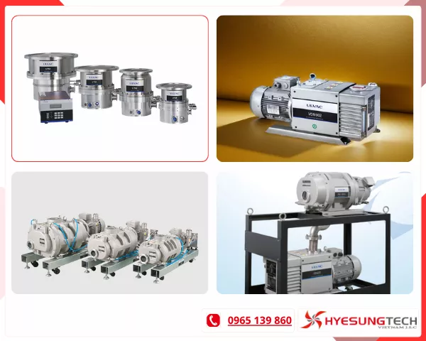
Các loại bơm chân không khô cao cấp là dòng bơm được sử dụng phổ biến nhất trong các nhà máy bán dẫn hiện đại do không sử dụng dầu trong buồng nén, giúp loại bỏ nguy cơ nhiễm bẩn dầu vào buồng xử lý. Loại bơm này đặc biệt phù hợp cho các công đoạn nhạy cảm như deposition, etching, ALD, PECVD, wafer handling và lithography. Ngoài ưu điểm về độ sạch, bơm khô còn có khả năng xử lý khí process, hơi ẩm và các sản phẩm phụ của phản ứng tốt hơn so với bơm dầu, đồng thời cho phép kết hợp hiệu quả với turbopump để đạt chân không cao và ổn định trong suốt quá trình sản xuất.

Một số dòng được ưa dùng như: Leybold DRYVAC DV 650 S, Leybold DRYVAC DV 300… Nếu có nhu cầu mua sắm vui lòng liên hệ
Turbomolecular pump
Turbopump là thiết bị tạo chân không cao, thường được lắp trực tiếp trên buồng xử lý nhằm đạt được môi trường chân không rất sạch và ổn định. Trong semiconductor, turbopump được sử dụng rộng rãi trong các công đoạn như PVD, dry etching, ion implantation, wafer handling và inspection. Do turbopump không thể hoạt động độc lập ở áp suất khí quyển, chúng luôn cần một bơm backing (thường là bơm khô) để hút sơ cấp.
Sự kết hợp giữa turbopump như Leybold TURBOVAC i/iX và bơm khô giúp đạt được dải áp suất từ chân không thấp đến chân không cao, đồng thời đảm bảo thời gian pump-down nhanh và độ lặp lại tốt giữa các chu trình.
Cryogenic pump
Cryopump là dòng bơm chân không cao hoạt động dựa trên nguyên lý làm lạnh sâu để giữ các phân tử khí trên bề mặt lạnh. Trong sản xuất bán dẫn, cryopump thường được sử dụng cho các ứng dụng yêu cầu môi trường cực kỳ sạch, đặc biệt trong PVD sputtering và một số quy trình deposition cao cấp. Ưu điểm nổi bật của cryopump là khả năng tạo chân không rất cao và giảm tối đa nguy cơ nhiễm bẩn. Tuy nhiên, loại bơm này cần chu kỳ regeneration định kỳ để giải phóng khí đã hấp thụ, do đó việc lựa chọn cryopump thường gắn liền với yêu cầu công nghệ cụ thể và kế hoạch vận hành của nhà máy.
Nếu nhà máy cần loại bơm này có thể tham khảo Leybold CRYO Torr Series.
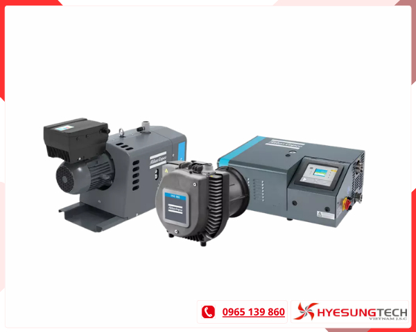
Bơm backing / bơm sơ cấp
Bơm backing hay còn gọi là bơm sơ cấp, có nhiệm vụ hút buồng từ áp suất khí quyển xuống mức áp suất đủ thấp để turbopump hoặc cryopump có thể hoạt động hiệu quả. Trong semiconductor, bơm backing hầu hết là bơm chân không khô, nhằm đảm bảo độ sạch và tránh hồi dầu. Bơm backing đóng vai trò quan trọng trong việc rút ngắn thời gian pump-down, tăng throughput và duy trì sự ổn định của toàn bộ hệ thống chân không, đặc biệt tại các load lock và transfer chamber.
Một số dòng bơm chân không cho sản xuất chíp và linh kiện điện tử nên dùng như: Leybold DRYPOINT, Atlas Copco GHS VSD+ Series.
Roots booster
Trong những hệ thống yêu cầu lưu lượng hút lớn và thời gian pump-down rất nhanh, bơm Roots thường được sử dụng để tăng hiệu suất hút ở vùng áp suất trung gian. Trong ngành bán dẫn, Roots booster thường được lắp giữa turbopump và bơm backing hoặc kết hợp với bơm khô trong các hệ thống có buồng lớn, nhiều load lock hoặc yêu cầu throughput cao. Việc sử dụng bơm Atlas Copco Roots giúp cải thiện đáng kể tốc độ hút mà không làm ảnh hưởng đến độ sạch của hệ thống.
Tiêu chí chọn bơm chân không cho chip & linh kiện điện tử
Chọn bơm chân không cho ứng dụng semiconductor không thể mua theo “công suất càng lớn càng tốt”. Môi trường sản xuất chip, bơm phải đáp ứng đồng thời mức chân không,độ sạch, độ ổn định, khả năng xử lý khí process và tối ưu throughput – yield. Dưới đây là các tiêu chí quan trọng nhất để chọn đúng cấu hình.
Dải áp suất mục tiêu và độ ổn định áp suất
Tiêu chí đầu tiên là xác định mức chân không cần đạt cho từng công đoạn. Ví dụ công đoạn load lock thường ở vùng chân không sơ cấp hay trung bình, trong khi ion implantation hoặc một số etch có thể cần chân không cao.
Nhà máy cũng cần để ý đến độ ổn định áp suất trong suốt chu trình. Nếu áp suất dao động, lớp phủ có thể không đồng đều, tốc độ etch thay đổi, dẫn rằng sai lệch CD và giảm yield. Vì vậy, ngoài đạt được áp suất, cần đánh giá khả năng “giữ áp suất ổn định” khi có tải khí liên tục.

Throughput và thời gian pump-down
Trong sản xuất hàng loạt, hiệu quả không chỉ nằm ở thông số chân không cuối, mà ở tốc độ đạt chân không và khả năng phục hồi áp suất nhanh giữa các chu kỳ. Buồng load lock, transfer chamber và các tool có cycle nhanh thường yêu cầu pump-down rất ngắn để tránh “kẹt nhịp” toàn dây chuyền. Khi chọn bơm, cần tính theo thể tích buồng, độ dẫn đường ống, vị trí lắp đặt và mức rò rỉ cho phép. Những yếu tố này quyết định pump-down thực tế, thực tế nó quan trọng hơn con số lưu lượng ghi trên catalogue.
Độ sạch và nguy cơ nhiễm bẩn
Sản xuất chip và linh kiện điện tử, phải sạch hoàn toàn. Do đó, nhiều ứng dụng ưu tiên bơm khô để tránh nguy cơ dầu bay hơi, hồi dầu hoặc tạo màng bẩn trong buồng.
Tính chất khí process và sản phẩm phụ
Mỗi công đoạn sẽ có đặc tính khí khác nhau: khí ăn mòn, khí độc, hơi ẩm, hạt/cặn phản ứng… Những yếu tố này quyết định việc chọn dòng bơm chân không cho sản xuất chíp phù hợp và các phụ kiện bắt buộc.
Nếu bơm không được thiết kế để xử lý các sản phẩm phụ, cặn bẩn sẽ tích tụ bên trong bơm, làm bơm hút yếu đi nhanh chóng, phải dừng máy để vệ sinh hoặc sửa chữa thường xuyên, từ đó gây gián đoạn sản xuất và làm giảm tỷ lệ sản phẩm đạt chuẩn. Trong thực tế, chọn bơm cho semiconductor là chọn khả năng xử lý tải khí cộng độ bền hóa học và chiến lược bảo trì chứ không chỉ chọn “độ chân không”.
Cấu hình hệ thống
Bơm chân không cho sản xuất chíp và linh kiện điện tử cần turbopump hoặc cryopump gắn trên chamber để đạt độ sạch và chân không sâu, đồng thời cần bơm backing đặt ở basement để hỗ trợ.
Hệ thống chân không cần được bố trí hợp lý về đường ống, van và điều khiển. Nếu đường ống quá nhỏ, quá dài hoặc nhiều co cút, dòng khí sẽ bị cản trở, khiến thời gian hút chân không kéo dài. Khi đó, dù bơm đúng thông số kỹ thuật, hiệu suất tổng thể vẫn thấp và áp suất khó ổn định.
Kiểm soát rò rỉ và độ kín hệ thống
Trong semiconductor, một rò rỉ nhỏ cũng có thể làm hỏng quá trình hoặc giảm tuổi thọ thiết bị. Vì vậy, tiêu chí chọn bơm phải đi kèm kế hoạch leak check định kỳ, khả năng duy trì chân không khi tải thay đổi và độ tin cậy của seal/valve/piping. Đặc biệt ở ion source hoặc các công đoạn nhạy, yêu cầu kiểm soát leak chặt chẽ và quy trình kiểm tra chuẩn là điều kiện bắt buộc để ổn định chất lượng sản phẩm.
Yêu cầu an toàn và xử lý khí đặc biệt
Một số công đoạn như EUV có thể liên quan đến lưu lượng H₂ lớn, hoặc nhiều tool yêu cầu N₂ purge đạt chuẩn quá trình sản xuất để bảo vệ bơm và ổn định quy trình. Khi đó, tiêu chí chọn bơm không chỉ là hiệu suất hút mà còn là khả năng xử lý khí dễ cháy, dễ phản ứng, vật liệu tương thích, cảm biến, giám sát và giải pháp xả xử lý an toàn theo tiêu chuẩn nhà máy.
Hyesungtech cung cấp bơm chân không chuyên dụng cho sản xuất chíp và linh kiện điện tử

Đối với ngành sản xuất chip và linh kiện điện tử, hệ thống bơm hút chân không là thiết bị phụ trợ ảnh hưởng cốt lõi quyết định chất lượng sản phẩm, tỉ lể đạt chuẩn sản phẩm và năng suất xử lý tổng thể của cả dây chuyền sản xuất trong một khoảng thời gian nhất định. Hiểu rõ yêu cầu khắt khe này, Hyesungtech Vietnam cung cấp các giải pháp bơm chân không chuyên dụng, đáp ứng đầy đủ các tiêu chuẩn kỹ thuật của ngành bán dẫn hiện đại.
Hyesungtech hiện là đại diện phân phối chính thức các dòng bơm chân không của Leybold và Atlas Copco, đáp ứng đa dạng nhu cầu từ chân không sơ cấp đến chân không cao.
Với kinh nghiệm triển khai thực tế tại các nhà máy điện tử và bán dẫn quy mô lớn như Intel và Samsung, Hyesungtech tư vấn giải pháp tổng thể từ lựa chọn cấu hình bơm, thiết kế hệ thống đến vận hành và bảo trì dài hạn. Chúng tôi cung cấp các dòng bơm chân không phù hợp cho từng công đoạn quan trọng trong sản xuất chip và linh kiện điện tử như deposition, etching, ion implantation, wafer handling, lithography và inspection. Các giải pháp được thiết kế nhằm đảm bảo độ sạch cao, áp suất ổn định và thời gian pump-down ngắn, giúp nâng cao hiệu quả vận hành.
Bên cạnh việc cung cấp thiết bị, Hyesungtech còn mang đến dịch vụ kỹ thuật trọn gói bao gồm:
- Tư vấn lựa chọn bơm và cấu hình phù hợp với từng dây chuyền sản xuất
- Kiểm tra hệ thống chân không, đo dò hở chân không và đánh giá hiệu suất vận hành
- Bảo trì định kỳ và sửa chữa vơm hút chân không
- …
Mọi thông tin xin liên hệ:
Vacuum Services – Bơm hút chân không Hyesungtech
- Điện thoại ( ZALO, VIBER ) : 0965 139 860
- Email: thiennguyen@hyesungtech.com.vn
- Văn phòng giao dịch: 201 Đường Cầu Diễn, Phường Xuân Phương, Hà Nội
- Chi nhánh miền Nam: 265 Tỉnh lộ 15, Ấp 1, xã Phú Hòa Đông, TP. HCM